 A professional manufacturer of UVLED curing systems
Custom circle UV curing system
2610inner ring UV LED curing light source are widely used in industrial applications, providing fast and efficient curing for a range of materials
View detailsSearch the whole station
In 2025, the global optical communications industry will witness a landmark breakthrough. According to the latest data from market research firm Cignal AI, global shipments of 800G optical modules are projected to grow by 100% year-over-year in 2025, while 1.6T optical modules will officially enter their first year of commercial deployment, with annual shipments expected to exceed one million units. Amid this wave of technological advancement, the precision requirements for optical module manufacturing processes have reached unprecedented heights. Futansi UV LED curing equipment, with its compact and practical design, is emerging as an indispensable partner for precision manufacturing within the optical communications industry chain.
As the global AI arms race fueled by large language models such as ChatGPT continues to intensify, the demand for high-speed optical interconnects in data centers is growing exponentially. By 2025, the global optical module market is projected to exceed $23 billion, with 800G optical modules becoming the mainstream configuration for hyperscale data center interconnects, while 1.6T optical modules are being shipped in volume through next-generation AI server platforms such as NVIDIA’s GB200 NVL72. Against this backdrop, critical manufacturing processes within optical modules—including optical coupling, chip packaging, and fiber connections—place extremely high demands on the precision, efficiency, and consistency of curing adhesives.
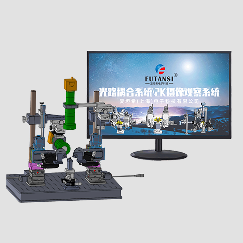
The manufacturing of optical communication components involves multiple precision curing scenarios: from bonding optical chips to substrates and coupling lenses to TO-CAN packages, to the precise alignment of fiber arrays with optical waveguides. Each step requires a UV curing process that is fast, uniform, and produces minimal thermal impact.
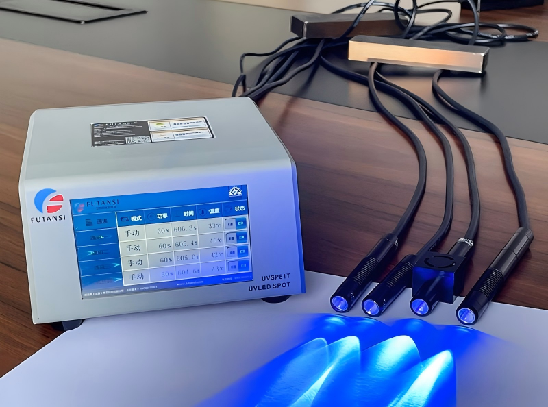
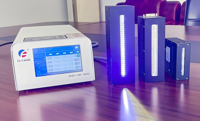
With its compact design and high-energy-density output, Futansi UV LED curing equipment perfectly meets the dual demands of space and efficiency on optical communication component production lines.
In the production of 800G/1.6T high-speed optical modules, the application of silicon photonics integration technology is becoming increasingly widespread. The precise coupling of silicon photonics chips with lasers and modulators requires the accurate curing of adhesives within an extremely short timeframe to ensure that optical alignment accuracy remains unaffected.
Futansi UVLED equipment’s high-energy-density output enables curing within seconds, while its low-temperature characteristics effectively prevent component displacement caused by thermal expansion, ensuring high-precision optical coupling.


inner ring UV LED curing light source are widely used in industrial applications, providing fast and efficient curing for a range of materials
View details
High-energy high-power water-cooled UV LED curing equipment is essential for large-scale industrial applications, providing fast and efficient curing for a range of materials.
View details
key aspects of UV flood curing systems
View details
HelloPlease log in