In the precision manufacturing chain of the liquid crystal display (LCD) industry, UVLED curing and processing technologies have already permeated multiple critical process steps.
Compared with traditional mercury lamp solutions, UVLED is reshaping the process standards of LCD production by virtue of its cold light source, instant on/off capability, pure spectrum, and energy-saving and environmentally friendly advantages.
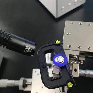
auto coupling system
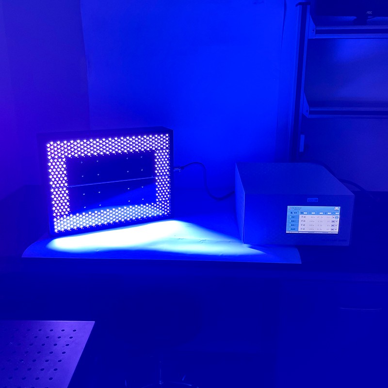
UVLED Photolithography Exposure: Precision Transfer of Micron-Scale Patterns
In the ITO conductive glass manufacturing process for LCDs, UVLED exposure is the core step of photolithography.
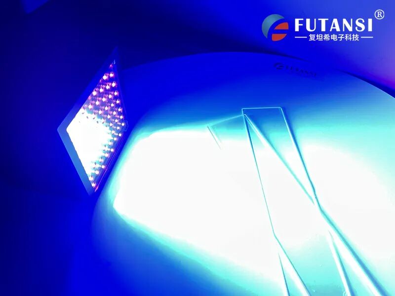
The principle is as follows: by selectively irradiating an ITO substrate coated with photoresist using ultraviolet light at specific wavelengths (typically 365 nm or 395 nm), a photochemical reaction occurs in the exposed resist film area, thereby altering its solubility characteristics in the developer solution.
Leveraging the high uniformity of UVLED light sources (energy uniformity up to ±3%) and their fast on/off characteristics, a steep solubility contrast can be formed between exposed and unexposed areas. Subsequently, using the photoresist as a mask, the ITO conductive layer undergoes selective wet etching, ultimately yielding high-precision electrode patterns on the glass substrate that correspond exactly to the photomask, laying the foundation for subsequent pixel driving.
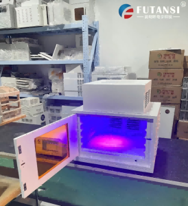
UV Curing Equipment for Optical Module Packaging
UVLED Surface Modification: Enhancing Interfacial Adhesion Between Films
In the production of display devices such as STN-LCD, the interfacial bonding quality between multi-layer thin films directly determines product reliability.
UVLED modification technology (ultraviolet surface property alteration) utilizes ultraviolet irradiation at specific wavelength bands to treat the surfaces of polymer film layers. Without damaging the substrate, it can:
Break surface polymer chains to generate active free radicals;
Introduce polar functional groups to increase surface energy;
Significantly enhance physical anchoring and chemical bonding between film layers.
This technology is widely applied to enhance adhesion at critical interfaces such as ITO conductive films and photoresist films, TOP coatings and PI (polyimide) alignment films, effectively resolving process defects like delamination and peeling.
UVLED Curing: Reliable Locking of Liquid Crystal Cell Encapsulation
The encapsulation and curing of liquid crystal cells (panels) is a critical process step to prevent liquid crystal leakage and isolate moisture and oxygen. UVLED curing systems undertake two core tasks in this stage:
1. Sealant (Frame Sealant) Curing After empty liquid crystal cells are laminated, UV-curable frame sealant needs to be applied along the borders. UVLED area or line light sources can uniformly irradiate large-area adhesive layers, achieving simultaneous surface drying and deep curing within seconds, while avoiding the thermal expansion and contraction issues of glass substrates caused by the thermal radiation of traditional mercury lamps.
2. End Seal Curing After liquid crystal filling, the injection port of the liquid crystal cell needs to be sealed. UVLED spot sources can precisely focus on the tiny sealing area to achieve localized rapid curing, avoiding photochemical damage to liquid crystal materials from ultraviolet light, while ensuring that the seal achieves airtight sealing strength (adhesion strength >15 MPa).
Photo-cleaning (UV Cleaning) technology utilizes high-energy ultraviolet light (usually combined with ozone generation) to excite organic contaminants on material surfaces to undergo photosensitive oxidative decomposition reactions.
UVLED light sources can thoroughly mineralize contaminants such as grease, flux residues, and silicones into volatile substances such as CO₂ and H₂O.
After UVLED photo-cleaning, glass substrates and ITO film surfaces can achieve “Atomic Cleanliness,” with surface contact angles significantly reduced, providing a contamination-free physicochemical interface for subsequent processes such as coating, gluing, and lamination, substantially improving product yield.
Futansi: A Trusted Partner for UVLED Curing Solutions
Futansi Electronic Technology has been deeply engaged in the UVLED curing field for over a decade, focusing on providing reliable curing equipment for high-end manufacturing industries such as optical communications, optoelectronics, new energy, automotive electronics, and PCBA.
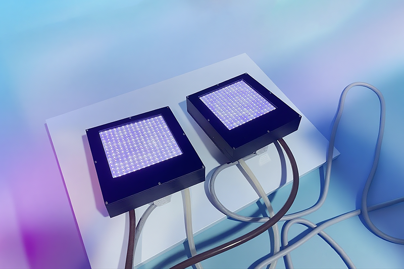
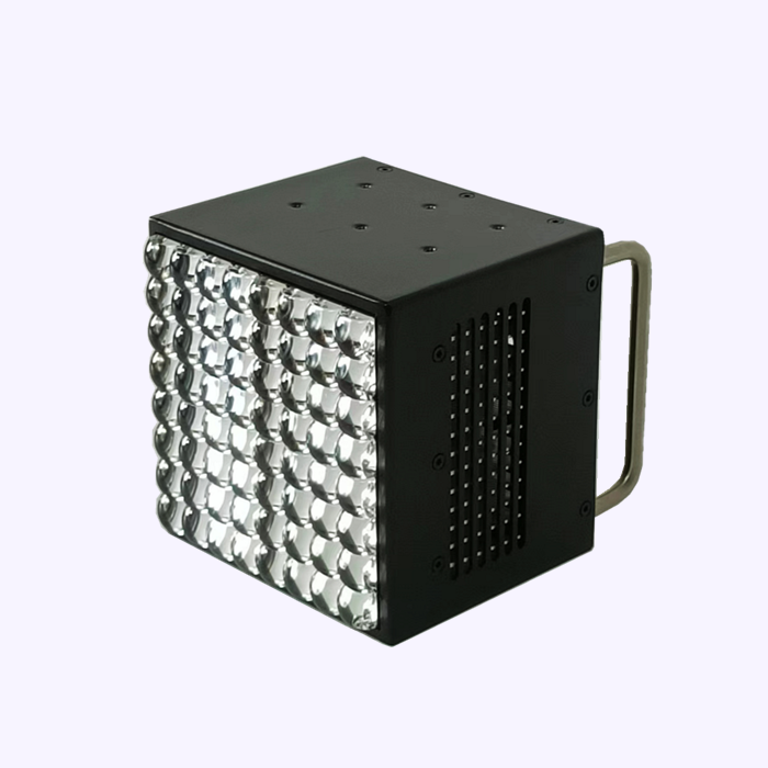
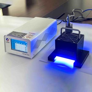
Our product portfolio covers UVLED spot sources, line sources, area sources, and intelligent curing conveyor systems, fully adapting to the exposure, modification, curing, and cleaning requirements of LCD production lines.
We provide free sample machine trials and customized solution design, equipped with a professional technical team offering full-lifecycle after-sales support to help customers achieve process upgrades and cost-efficiency improvements.
In production line deployment, it is recommended to pair with a 365 nm or 395 nm UVLED spot or area curing system, using a programmable controller to set a two-stage process of "low-irradiance pre-curing + high-irradiance full curing." This minimi...
In the UVLED curing equipment industry, many manufacturers invest heavily in thermal design simulations to ensure devices operate within safe temperature ranges. Yet one critical question often gets overlooked: what happens when temperatures rise ...
As optical transceiver modules evolve toward higher speed, miniaturization, and high reliability, the UVLED curing chamber has become standard equipment in optical communication manufacturing, leveraging core advantages of "cold curing, precise en...
UVLED curing technology is profoundly transforming manufacturing processes in the medical sector with its high efficiency, environmental friendliness, and precision. As professional UV curing equipment manufacturers, we are dedicated to providing ...
 A professional manufacturer of UVLED curing systems

HelloPlease log in